

Electronics Design Considerations for an Astrobee Payload: Robustness
Thomas Ziegler, Electrical Engineer
Approximate 8 to 15 minute read
This column, the first installment of a series, is intended to serve as a guide for the design of electronics bound for space, specifically as a payload on Astrobee (more on that later), with links to interesting and potentially useful resources, background information on the process of getting your electronics to the space station, and some etymological hot takes. This particular writeup will focus on robustness: how to make sure your beautiful electronic creation will survive the trip to space and live a prosperous life. To be clear, this column does not constitute engineering advice; rather, it is intended to be informative to the layperson and thought-provoking for a young engineer tackling their first space design. Every payload is unique and the discussion here is not an all-inclusive checklist of design parameters to address. With that said, let’s get into the good stuff!
Astrobee
Astrobee, a (very cute) robot on the International Space Station (ISS), was developed by the NASA Ames Research Center as a platform for doing cool science and useful tasks in space. Astrobee packs a lot into a small package: it uses fans and ducts to propel itself in any direction; it has a boatload of avionics and three onboard computers for sensing, navigation, and wireless communication; it includes cameras, a microphone, and even a laser pointer; and most importantly for KMI, it is designed as a platform to host other widgets, known as payloads. In the past, it has hosted physical payloads such as Australia’s Commonwealth Scientific and Industrial Research Organization (CSIRO) Multi-Resolution Scanning 3D mapping experiment, Stanford’s gecko adhesive gripper, and University of Southern California’s CLINGERS docking hardware, as well as software payloads like the Naval Postgraduate School’s Astrobatics guidance and control model. KMI’s REACCH demo is also an Astrobee payload, and this column aims to discuss some of the design considerations made in and lessons learned from the process of designing REACCH electronics.

Figure 1: Astrobee free-flyer robot on the ISS. Image credit: Space.com
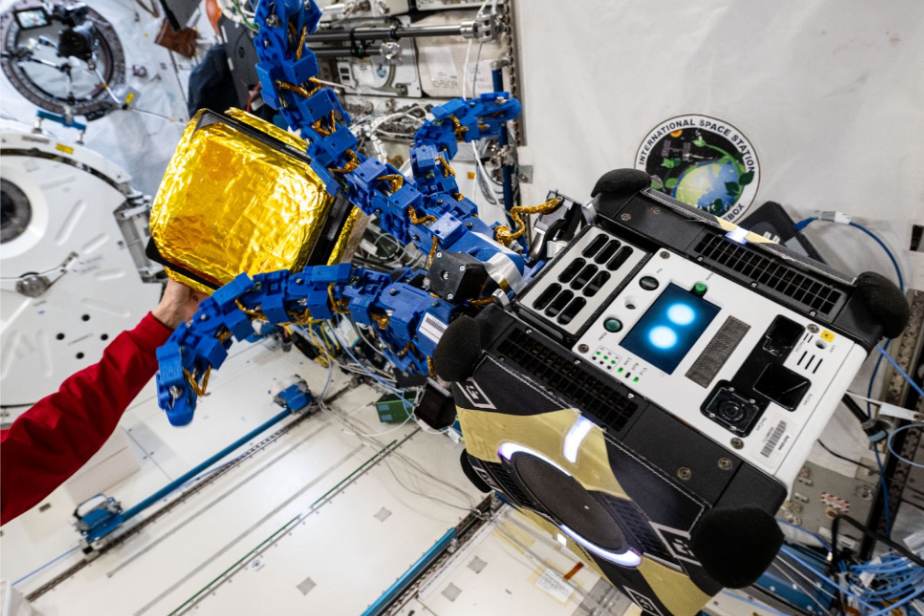
Figure 2: Astrobee REACCH grappling a target cube. Image credit: NASA
As an Astrobee payload developer, there are lots of good resources available to you. Make sure to ask your Payload Integration Manager (PIM) for the PIM Roadshow slides, an excellent summary of the whole payload development process. For Astrobee specifics, this webpage has lots of good links, including the Guest Science Guide (an absolute must-read), the software Github (and corresponding internal software wiki), and an overview of the systems engineering design. Also make sure to get the payload connector pinout.
SSP 57000
Any payload hosted on the ISS needs to follow the rules, primarily SSP 57000, a requirements document which specifies all manner of things your payload must do and not do, from structural resilience to the materials used to how it connects to the network to how loud it is. You will be assigned a Payload Interface Requirements Engineer (PIRE) who helps determine which requirements are relevant to your payload, and a safety panel will determine if your payload contains any safety-critical structures or circuits, in which case additional requirements will be levied. By virtue of being an Astrobee payload, a lot of the power, isolation, and communications protections have been done for you, which eases the requirements burden as a payload developer, but your PIRE has the final say in what requirements you need to meet.
The International Space Station
The ISS microgravity environment is a nice middle ground between the ground and space. On the ground, if something doesn’t work it can be serviced by humans; in space, that’s not an option. On the ISS, there are crew members available who can help debug and troubleshoot, but their time and access to tools are very limited. Just like when designing for a full space environment, the electronics need to survive the rocket trip up and work reliably when they arrive.
Getting Zapped
Electronic devices are usually pretty resilient, but one surefire way to kill them is to accidentally give them too much voltage, which is basically a measure of oomph for moving electrons. Some voltage is necessary to make electric current flow in a circuit, but too much of it will cause insulating materials to break down and start allowing current to flow to places you don’t want it, likely causing a cascading failure. Let’s talk about some over-voltage risks and mitigations.
ESD Protection
Any voltage-sensitive electronics, especially anything that will be touched by crew or interfaces with the outside world, should be protected from electrostatic discharge (ESD) or “static shock”, per SSP 57000 3.2.2.6. Electrically, ESD looks like a large amount of charge deposited in your conductor in a short amount of time, and if the charge has no place to go it can build up voltages in excess of 10kV, so the trick is giving the charge a low-impedance path to dissipate quickly. Altium has an overview, as does Cadence, of some basic ESD protection strategies, and Microtype has some nice SPICE simulations of protection circuits in action.
Debris
Most electronics have a maximum voltage they can tolerate. It is very common to have a single device using multiple different voltage domains, like an Astrobee payload which takes the unregulated Astrobee battery voltage (~14 V) and regulates it down to 5V. You need to take care that the low-voltage stuff doesn’t touch the high-voltage stuff, otherwise you’re going to have a bad time. Usually this is done by keeping voltage domains physically separated and electrically insulated. However, in microgravity, things like to float around, including conductive solids and liquids which will happily bridge the gap and conduct 14V straight into your sensitive components. This is one reason why humidity and debris on the ISS is precisely controlled (SSP 57000 3.12.3.1.1). Still, there is always the risk that debris gets into your electronics enclosure, whether the debris come from somewhere else or are created by breaking or abraiding material in your own payload. You can protect your electronics with conformal coating, potting, or hermetic sealing, preventing something conductive from floating around and ruining your day.
Power
Most payloads on the ISS will be powered by the 120V or 28V supplied by the ISS’s electric power system, which includes solar panels, batteries, and electronics for distribution and monitoring. In order to be a good neighbor, a payload connecting to a shared power bus will need to, among other things:
Tolerate and protect itself from a wide range of voltages on the power bus (SSP 57000 3.2.1.3, 3.2.2.2).
Control return currents very strictly (SSP 57000 3.2.1.4).
Use overcurrent protection, in the form of a fuse or circuit breaker, to prevent itself from consuming more power than the ISS power system can supply (SSP 57000 3.2.1.2).
Minimize conductive susceptibility and limit conductive emission (SSP 57000 3.2.2.2). This will be discussed in a future column but the general idea is “tolerate noise from your neighbors on the power bus while not making noise yourself”.
Luckily, Astrobee has already done a lot of the work for you.
Voltage Tolerance
Astrobee can be commanded to connect a payload to its battery. Battery voltage is nominally 14.4V, but the Astrobee Guest Science Guide indicates that payloads should tolerate at least 11-17V as the batteries discharge throughout the mission. It’s still good practice to design your payload to handle voltages well outside this range–see for instance the overvoltage section in the appendix–but Astrobee’s batteries isolate your payload from the rest of the ISS’s communal power which makes your life easier.
Return Currents
“Return current” refers to the idea of electricity flowing in a circuit–in general, if your circuit is shoving electrons in one direction (supply current), there will be an equal number flowing back the other direction (return current)[1]. In a car, the metal frame is used as a general-purpose conductor to return current to the battery; you use wires to get the electrons from the battery to the device requiring power and trust the electrons to find their way back home through the frame. On the ISS, that won’t fly. Any conductor with current flowing one direction in the payload needs to be paired with a conductor for the current to come back. There is a single connector in an Astrobee payload bay that supplies power and digital communications to your payload. This makes return current discipline easy as the current flowing out of the connector into your payload has to flow right back through the same connector.
Overcurrent Protection
“Overcurrent protection” usually takes the form of a fuse or a circuit breaker, something to detect when a device is consuming too much current and interrupt the flow, cutting off power. A common misconception about fuses and circuit breakers is what they are intended to do. If a device is consuming more current than it was designed for, chances are that device is already broken; the job of overcurrent protection is to limit the collateral damage. In you house, for instance, circuit breakers protect the wires in your walls from conducting more current than they were designed for, overheating, and starting a house fire. Since a potential fire on the ISS is a huge concern, overcurrent protection is a must. Astrobee uses a current sense amplifier to monitor the current flowing to each payload and will disconnect a payload drawing more than 3A, so overcurrent protection for your payload is built-in[2].
PCBs and Hardware Design
When designing for a space environment, there are many environmental factors for your electronics to deal with including vacuum, heat dissipation, and thermal cycling. As long as you get a spot in the pressurized portion of an ISS resupply capsule, your Astrobee payload ISS should not have to deal with any of these conditions, which is mighty nice. The main concerns for an Astrobee payload are things like surviving the shock and vibration of launch, protecting from free-floating debris, making the human interface simple and foolproof, minimizing electromagnetic interference (EMI), and to a lesser degree radiation tolerance. We will discuss a few points below.
Printed circuit boards (PCBs) are ubiquitous in the electrical engineering world as a wonderful way to make the electrical connections between components compact, robust, and easy to manufacture. However, as with any scheme for selective electrical conduction, they have limitations, some of which will be discussed here. NASA also has a quick reference for PCB design considerations, referencing lots of different standards.
Acceleration, Shock, and Vibration
The art of designing and fixturing devices to survive a rocket launch is a whole field of expertise in itself. From your payload’s perspective, the experience is positively apocalyptic. For a few minutes after the first stage ignites, everything in your payload is accelerating very quickly, which from your payload’s point of view feels like gravity is pulling down at least four or five times as strongly as usual. The rocket also vibrates like there’s no tomorrow, so your payload is also contending with a continuous earthquake, punctuated by sporadic jolts–shocks–of force during events like stage separation and fairing deployment. Testing for this environment is colloquially known as “shock and vibe” and it takes a lot of care to make anything, especially delicate electronics, survive.
Surviving the acceleration is mostly about reducing mass and careful fixturing. Mass reduction is always a goal in spaceflight because each gram of payload costs more propellant in the launch vehicle, but in particular during high acceleration, lighter components require less force to move[3]. Fixturing is a bit more nuanced. Circuit boards, which are basically thin fiberglass sheets, should have mounting holes placed so that there are no long unsupported spans; the shorter the span, the less it will flex from static acceleration, and flexing is what tends to kill circuits during launch. The failure mode is fun to illustrate (see Figure 3) but difficult in practice to prevent: any time the board experiences a force applied to its mounting points, the unsupported span will bend. Bending stresses the solder joints[4], as shown in Figure 3, and with enough stress the solder joint will crack, inhibiting the flow of current and disrupting the circuit.

Figure 3: PCB flex (exaggerated) stresses solder joints, leading to failure
PCBs aren’t the only thing to think about. Wire bundles should be held in place (“staked”) at regular intervals to keep them from flopping around. You can find recommended staking distances in NASA’s workmanship handbook. Importantly, you can choose how your payload is oriented in the rocket and as such what direction is up: take advantage of this choice! The structure only needs to withstand the acceleration in one direction.
While static acceleration is straightforward to account for, handling shock and vibration is another matter. Shock, a sudden impulse of force[5], can result in huge instantaneous accelerations, shaking, breaking, misaligning, and dislodging components. Vibration (SSP 57000 D.3.1.2) is historically responsible for a good number of first-day spacecraft failures, causing all sorts of mechanical failures, and electronics are no exception. Any mechanical structure will exhibit resonance for certain frequencies of vibration, where a small shaking force will result in a relatively large deflection or bending. In general, rocket launches tend to have the strongest vibrations below 100 Hz, so it is a general rule of thumb to keep mechanical resonant modes above 100 Hz for anything going on a rocket. Different rockets will create different vibrations, and launch providers will often specify exactly what to expect. See for example SpaceX’s Falcon User’s Guide, which specifies a vibration spectrum on page 19.
Resonant peaks can be moved to a higher frequency by reducing the length and increasing the stiffness of unsupported spans of anything, like wire bundles or PCBs as discussed above. After addressing resonance, you can do some additional vibration damping[6]. Vibration-sensitive devices can be isolated on rubber bumpers. Astrobee REACCH had a cushy ride to space in custom-molded foam, and for many ISS payloads bubble wrap is sufficient. There are some other tricks for protecting your electronics, as discussed in the appendix.
Component Selection
After making sure your components don’t rattle loose, it’s time to talk about the components themselves. There’s plenty to talk about, so this paragraph will cover the main points. EEE-INST-002 is the general NASA standard for component selection which covers just about everything. NASA also provides the NASA Electronic Parts and Packaging program (NEPP) which has among other things a list of military performance standard (MIL-PRF) components that meet INST-002 standards. For a payload developer with a focus on reliability and a big budget, MIL-PRF parts are as rugged as they come, subject to a whole battery of tests[7] to ensure they will survive harsh mechanical, electrical, and radiation conditions. However, that reliability comes at a design cost, and an Astrobee payload can be built with more common parts. There is also a useful NASA guideline on derating components[8], which is generally just good advice for designing any reliable electronics.
Conclusion
This has been a first installment in what will hopefully be a series of columns on electronics. In the next I hope to cover electromagnetic interference and electromagnetic compatibility
(EMI/EMC). Until then, keep your noise floor low and your factor of safety high. Here’s to keeping space clear for all!
[1] I somewhat flippantly describe electric current as “shoving electrons around”. This is something of a simplification; electric current as we usually think about it is the apparent motion of electron vacancies. A vacancy, known by the ever-creative physicists as a “hole”, is a space an electron leaves behind when it moves from the valence orbital of one atom into an available hole in another atom. Electrons themselves move slowly but holes can propagate at the speed of light.
[2] This is speculation but I’m fairly sure there’s a lot of software in the overcurrent detection process, so there may be at least several milliseconds of delay between current consumption crossing the 3A threshold and Astrobee disconnecting power. This is still significantly better than most fuses or breakers, which depending on their design may take seconds or minutes to trip. In any event, Astrobee provides overcurrent protection for your payload, making your job easier.
[3] Newton’s second law of motion says that the force F required to move a mass m through an acceleration a is F = m a. More mass takes more force to move, and that force has to be delivered via stress in materials from the engine of the rocket all the way to the payload. By reducing the mass of a single resistor in your payload, you’re reducing the stress in the PCB it’s on, the screws holding the PCB, your chassis, and every load-bearing part of the launch vehicle. For a somewhat related historical example, see Real Engineering on the WWII development of the proximity fuze.
[4] Solder is a soft metal often used to make mechanically sturdy electrical contact between the lead of a component and the pad of a PCB By heating the lead and pad, the solder is able to liquify and chemically bond with the contacts, forming a solid, conductive joint Solder is easy to use and easily reversible for electronics repair but has some limitations in space; in addition to cracking, lead-free solder (which is primarily tin) tends to grow “whiskers” which cause trouble For the Apollo missions, many joints were welded instead of soldered for a more robust connection, as shown in Ken Shiriff’s beautiful blog article.
[5] Interestingly, a perfect impulse mathematically contains components of all frequencies, so the truly pedantic can insist that shock is just a special case of vibration Either way, it’s a cool test that usually involves a big, very scientific hammer.
[6] My college roommate had a professor whose pet peeve was the misuse of the term “dampening” “You can’t dampen vibrations!” he would say, “how on earth would you pour water on a physical phenomenon It’s damping, you damp vibrations!
[7] In general, this kind of rigorous testing on every component is not practical for manufacturing a large number of units, like in the automotive industry which cranks out millions of cars in a year. Manufacturing for space where, especially in the case of an Astrobee payload developer, the quantity of units is often single-digits, tends to prioritize reliability over part cost reduction. At the moment, it is almost impossible to reasonably fix something once it’s left the ground, and exceptions like correcting the Hubble optics wind up being enormously expensive. As they say, a gram of prevention in low earth orbit is worth 23 grams of propellant on a Falcon 9.
[8] “Derating”, a fascinating term not unlike the aviation industry’s “pre-boarding”, means using a component below its maximum rating, e.g. a 14.4V voltage rail is buffered by a capacitor rated for 25V, giving a derating factor of 14.4 / 25 = 0.58, within the NASA-suggested 60% maximum derating. For Astrobee REACCH, I ran 50V-rated caps on the unfiltered Vbatt input and 35V on the filtered side.
Appendix Stuff
This appendix contains some more technical tidbits intended for a reader with some electronics background and an interest in space applications. Again, these are some thoughts and tidbits I hope will be helpful, so please don’t construe it as engineering gospel.
ESD Protection
Most of the extra ESD content consists of the things I wish had been covered in EE3131 Intro to Electronics. To be clear, I am not a particularly experienced hardware designer so most of this is either things that worked at my old job designing a particle accelerator or general wisdom I’ve heard or read about.
Transient Voltage Suppressors
The bread and butter of ESD protection are transient voltage suppressor (TVS) diodes. TVS diodes are basically specialized Zener diodes, and the schematic symbol may be similar or identical, but the intended use is different. Zeners are designed for continuous use above the reverse breakdown voltage for smoothing voltage transients, whereas TVS diodes are intended for use below the reverse working maximum voltage VRWM, and during nominal operation behave like an open circuit. TVSs have a much lower parasitic capacitance, allowing for a much faster response to a sudden change in voltage, and can sustain their peak pulse current for a short time. As voltage from anode to cathode grows more negative, the TVS reaches its breakdown voltage VBR and begins conducting current, until reaching the maximum design current IPP at clamping voltage VCL. A bidirectional TVS exhibits the same behavior for a positive voltage, whereas a unidirectional TVS behaves like a normal diode in forward bias, conducting at a positive forward voltage VF.00

Figure 1: Unidirectional TVS diode I-V curve

Figure 2: Bidirectional and unidirectional TVS diodes
It’s common to insert a single bidirectional TVS between a conductor to protect and ground (D2 below). During an ESD event, the voltage on the conductor will be clamped to within ±VCL. This is sufficient for many devices and for bipolar signals (e.g. audio) which may range positive and negative relative to ground. However, many digital logic signals range from ground to the positive supply voltage (unipolar), and most logic integrated circuits (ICs) can only tolerate a small negative voltage (~0.3 V). A common solution is to place a unidirectional TVS (D3 below) with a working voltage VRWM equal to or greater than the logic high voltage VDD. In this case, the diode will clamp the voltage to +VCL and a bit past -VF.
This is pretty good, and is sufficient protection for lots of applications, but there may be some problems. For most TVSs, +VCL may be well above +Vmax for devices downstream of the ESD protection. Adding a second unipolar TVS (D1) will help clamp the voltage to VDD + VF. One point of note is that VF only applies to low forward currents, and a forward surge current may push the voltage higher. If the downstream devices have a low current consumption and are particularly sensitive to voltages outside the range 0-VDD, a resistor (R1) and a second stage of Schottky diodes (D5 and D8) can be added; the Schottkies clamp the voltage very close to their VF since the resistor limits the forward current. The second stage diodes are overkill and can be omitted for most applications, as modern IC packages have protection diodes built-in.

Figure 3: Various TVS configurations
Diodes are the simplest building blocks of ESD protection, but there exist other methods for protecting electronics from overvoltage events. Cadence has an overview of some transistor-based approaches; my understanding is that this kind of circuit is better suited in power supply electronics to prevent catastrophic failure modes or at the power input to your electronics to prevent damage from a voltage surge, but I’ll discuss some options for completeness.
MOSFETs
A transistor like a MOSFET may be used for overvoltage protection, but be careful. Remember, if you don’t give ESD charge a place to go it will build up to an obscenely high voltage, so while I have no experimental proof personally, I think that even if your comparator circuit reacts fast enough to the sudden rise in voltage and cuts off the circuit, the huge voltage will well exceed most transistors’ VDS, max and blow up your protection circuit.
Crowbar Circuits
So far, the approaches to overvoltage protection rely on clamping the voltage to some maximum and shunting current through a protection device to keep it that way. A more nuclear approach is the crowbar circuit (a goofy name; I thought for sure the Art of Electronics would have the origin of the name but the best I can find is the Wikipedia explanation) which monitors the voltage on a line and if it exceeds a threshold, a silicon-controlled rectifier (SCR) shorts the line to ground, protecting downstream components by lowering their supply voltage to near zero and hopefully tripping overcurrent protection upstream. Figure 4 shows a simple crowbar circuit wherein as the input voltage rises, the Zener diode D9 will begin to conduct above some breakdown voltage VBR. After the voltage rises a few hundred millivolts above VBR, R2 is conducting enough current that the SCR is tripped into conduction, shorting the output to ground and blowing the fuse.
As mentioned in the section on current-limiting, I’m fairly sure Astrobee digitally monitors payload current consumption and will disconnect power if the payload consumes more than 3A (see page 8 of the Astrobee EPS board schematic if you have access) but being software-controlled, the response time is likely not deterministic nor guaranteed.

Figure 4: a very simple crowbar circuit
Current Path
The components used are only half the battle for ESD protection; the entire current path needs to be low-impedance to keep the voltage experienced by electronics low, because for a given surge current i(t), a higher total resistance R will allow a higher voltage V to build up following V=Ri and higher inductance L will result in a voltage spike as the current ramps up quickly, following V=L di/dt. For PCB design, placing ESD protection near the point where surge current enters helps keep the parasitic inductance low. Using a ground plane (and connecting to it with one or more vias) also helps provide a low-inductance path for the charge to dissipate.

Figure 5: Section view of current flowing through a TVS diode
PCB Design
Here are some additional thoughts regarding PCB resilience. While thermals and pressure in a vacuum are not a concern for an Astrobee payload in the luxurious, air-conditioned cabin of the ISS, I’ve included some thoughts for reference.
As a sidebar, when prototyping PCBs, it is tempting to baby your creations and treat them gently. I recommend you don’t! Press down on them in the direction of acceleration, toss them around on the bench, and any failures you discover are potential mission-killers you just prevented. Similarly, when testing the function of your devices, don’t shy away from sending all the inputs to the rails[9], toggling settings randomly, and generally trying to push the limits of all the things you’re worried about breaking to make sure they don’t or fix them if they do. I will stress, I think it’s good to push the mechanical limits of your prototypes, not the final flight hardware, which of course you’ll want to treat with care.
Vacuum
Space is, famously, a vacuum–a region of the universe mostly devoid of matter. There are basically no gas molecules bonking around, giving rise to the phenomenon of atmospheric pressure, like there are on the Earth. For most electronics, operating in a vacuum is mostly not a problem[10]. The trick is making the transition from one atmosphere of pressure to zero atmospheres in space. Any enclosed cavity which contains air on the ground either needs to be sealed to prevent leakage or allowed to vent as the rocket gains altitude and the ambient pressure decreases. Normally this is a problem for mechanical engineers to figure out–the vent hole needs to be sized appropriately to set the flow rate for a given volume cavity and a given rate of change of pressure–but for EEs it matters in components like electrolytic capacitors. Most electrolytic caps have vent plugs that are intended to blow out if the electrolyte starts to boil, and this will most likely pop if you sent it to space, spewing gas into your electronics and allowing the electrolyte to evaporate, deteriorating capacitor performance. Bottom line: look out for enclosed cavities in your parts, no wet electrolytes if you can help it, and make sure the package is hermetically sealed if you can’t.
Thermals
For most electronics, operating in a vacuum is mostly not a problem. The exception is usually thermal management. On Earth, you can rely on convection to dump heat from your components into the air around you, a generally effective way to keep power-hungry components cool. In vacuum, the only passive ways to cool your parts are conduction through your board and wire harnesses, which works okay until the board and wires heat up too, and radiation, which is the only real way to get heat away from your spacecraft at all. In general, make sure you do thermal vacuum (T-Vac) testing on your electronics to make sure you’re getting heat away quick enough. Active cooling, usually in the form of cryocoolers and heat pipes, can move heat from your components, but it still has to get radiated into space somehow. My understanding is that nanosatellites generally don’t have a problem with getting too hot, but as your spacecraft grows in size, the square-cube law tends to mean you generate more heat than you can dissipate through the chassis alone, and a dedicated radiator may be necessary.
Also, thermal cycling is rough on PCBs. Most spacecraft in Low Earth Orbit (LEO) will experience a cycle of being irradiated by the Sun and eclipsed by the Earth every 90 minutes. This cyclical heating and cooling causes corresponding expansion and contraction of all materials, and that includes your electronics, specifically any two joined materials with different coefficients of thermal expansion. This includes the copper and fiberglass in PCBs, which can cause failures in vias which are blind, buried, or have a high aspect ratio; copper traces and plastic IC packaging, which can stress and crack solder joints, and even the woven fiberglass of most PCBs will have slightly different coefficients of expansion in the x and y axis, causing further stress on soldered components. So, while your boards are in the T-Vac chamber, don’t forget to do some hot-cold cycles while you’re at it.
Shock & Vibe
You can also support larger components like bulk capacitors with globs of hot snot (silicone adhesive) for additional stability and some vibration reduction. It’s probably wise to do this to any internal connectors, too. Potting is also a great way to make sure everything is held in place, and increases standoff voltages too. Just be aware that once you entomb your stuff, you’re probably never getting it back out! Even diagnosing failure can be tricky.
Component Selection, continued
Through-hole (THT) components tend to be generally more robust to mechanical disturbances than surface-mount (SMT), at the cost of increased complexity in PCB manufacturing and soldering as well as lower trace density on multi-layer PCBs. This is all because of the holes; holes are drilled one at a time, so more holes takes more time which costs more money. Fab houses can plate the holes simultaneously with a chemical process (check out this project which is trying to do via electroplating, one hole at a time, on a DIY setup), but then the components have to be soldered. SMT parts can be reflow soldered, which is great because you just need an IR oven and you have very precise control over how much heat the components take. THT parts can’t be reflowed (reflown?) and the common method is instead wave soldering, a wild process that involves passing the PCB over a small standing wave of molten solder. As you might expect, it’s pretty expensive and all that molten solder (especially if it is leaded) presents a safety risk.
Regarding military-grade parts, there’s no denying they’re rugged and will serve you well, but they may arguably make your life as an Astrobee payload developer harder. Take the MIL-PRF-39003 standard for tantalum capacitors for example. As of the writing of this column, of the 15,200 MIL-PRF-39003 compliant capacitor models in Digi-Key’s catalog, only 154 unique values are in stock, at a price between $8 and $90 per capacitor. These are also large components, available only in an axial leaded through-hole package, which limits how many you can fit on a board in an Astrobee payload bay. Additionally, a lot of the rigorous environmental requirements and testing, like 39003’s requirements for the liner being a nonfungal material and the capacitor’s resilience to thermal shock, isn’t strictly necessary for most Astrobee payloads. With some extra work you can pick and choose important parameters from the standards, match them with datasheet values, and open yourself up to more options.
There is some argument to be had over the performance of THT and SMT in harsh environments. My understanding is that having some kind of lead between the part and board (e.g. SOIC, QFP, or any through-hole part) allows for stress relief from length changes due to thermal cycling, while packages without leads like QFN and BGA will experience greater stress as temperature changes. In a high-acceleration or high-vibration environment, reducing mass is generally the best way to ensure survivability, giving SMT parts an edge yet again. The guidance I’ve seen is to generally stick to leaded SMT parts where possible, with some exceptions like connectors that humans will use.
Be aware that when choosing capacitors, there always exists a tradeoff in package size, capacitance, dielectric voltage/temperature linearity, and voltage rating. You can only shove so much performance into a given package, so if you’re having a hard time finding what you need, chances are just putting two smaller caps in parallel is the solution.
[9] A voltage “rail” is just a voltage supplied to power multiple devices. The term originated from old-school schematics, where the standard was to draw supply voltage connections as a big horizontal line from which devices tap off power (see the bold, horizontal lines in this LK-72A audio amplifier’s ground rail for example). Parallel lines on the schematic look kinda like railroad tracks, and even though the zeitgeist has moved away from that style of schematic, the name stuck.
[10] In fact, devices which rely on electron beams require a vacuum to function. This includes vacuum tubes, which sounds positively ancient and not at all space-age, but one area of space electronics where vacuum tubes still reign supreme is the Traveling Wave Tube Amplifier. TWTAs are still the best high-power, high-bandwidth amplifiers out there and are used in satellite transponders.
Recommended column to read next: 3D Printing and Space Manufacturing - One Layer at a Time